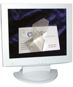
Invisicon® Carbon Nanotube Technology
Website
Date Added
1 January 2007
Country of Origin
Categories
“The secret to Invisicon™ is in the nature of Carbon Nanotubes. These remarkable structures allow us, through our proprietary purification and coating processes, to create unique conductive structures. Our conductive Nanotubes have roughly a 1000:1 aspect ratio, which gives us the ability to apply a very small amount of the material to achieve good conductivity, such a small amount that when applied to transparent films it does not significantly degrade light transmission.”
Supporting Info URL
"The search for the ideal transparent electrode for flexible displays in lieu of the brittle and expensive indium tin oxide (ITO) electrode continues. Single-wall carbon-nanotube (SWNT) coatings, especially on plastic films, are a viable alternative to ITO for flexible-display applications, offering superior durability and flexibility, ease of processing (wet coating and patterning), low reflectance, and neutral color" Peltola et al. (2007)
"Transparent and electrically conductive coatings and films have a variety of fast-growing applications ranging from window glass to flat-panel displays. These mainly include semiconductive metal oxides such as indium tin oxide (ITO) and polymers such as poly(3,4-ethylenedioxythiophene) doped and stabilized with poly(styrenesulfonate) (PEDOT/PSS). In this paper, we show alternatives to ITO and conducting polymers, using single-wall carbon nanotubes (SWNT). These CNT-based technologies offer conducting substrates having a broad range of conductivity, excellent transparency, neutral color tone, good adhesion, abrasion resistance, and flexibility. Additional benefits include ease of both processing and patterning. This paper reports on optoelectronic properties and structure characterization of these materials." Trottier et al. (2005)
Nanomaterials
Shape/Dimensions
Nanotube
Shape/Dimensions (source)
Functions of Nanomaterial
Location of Nanomaterial
How much we know
Additional Information